The 448G Architecture Shift: Breaking the PCB Barrier in AI Infrastructure
The rapid evolution of artificial intelligence is driving hardware engineering to achieve physical marvels that were considered science fiction just a decade ago. As AI models scale into the trillions of parameters, the infrastructure required to train them is demanding unprecedented bandwidth. The industry is currently moving through the 224 Gbps PAM4 transition and is already laying the architectural groundwork for 448 Gbps signaling.
To support these massive AI clusters, often referred to as scale up networks, the physical layer of the data center must evolve. We are witnessing a fundamental shift in how data is routed, driven entirely by the unforgiving laws of physics.
Here is a deep dive into why traditional circuit boards are hitting a hard limit, how advanced cabling architectures are solving the immediate bandwidth crisis, and what the ultimate future of On ASIC integration looks like.
The 110 GHz Wall: Why the Circuit Board is Maxing Out
To understand the shift in interconnect architecture, you have to look at what happens to an electrical signal at extreme frequencies.
To push data at 224 Gbps or 448 Gbps, the channel bandwidth must stretch into the millimeter wave spectrum, pushing up to 110 GHz and beyond. At these frequencies, traditional printed circuit boards, even those made with premium, ultra low loss materials, face severe physical limitations:
• The Skin Effect: At 110 GHz, the electrical current no longer travels through the entire copper trace; it gets pushed to the extreme outer surface. Any microscopic roughness on the copper trace causes the signal to scatter, creating massive insertion loss.
• Dielectric Absorption: The substrate material of the PCB acts like a sponge, absorbing the high frequency signal energy and converting it into heat.
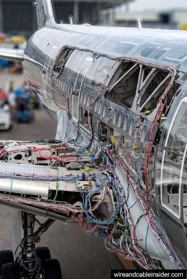
• The Distance Problem: At 10 Gbps, a signal can easily travel 30 inches across a motherboard. At 224 Gbps and bandwidths approaching 110 GHz, that reliable transmission distance shrinks to mere inches.
If a switch ASIC sits in the middle of a server board, the signal degrades into noise before it ever reaches the front panel ports. To cross a distance of even one meter, the signal must be lifted off the lossy PCB and routed through advanced twin axial wire or fiber optics.
Satisfying the Immediate Need: Flyover Architecture
For data centers that need to deploy massive 224G and 448G infrastructure today, tearing up server architecture to mount fiber optics directly onto silicon is a complex and costly proposition.
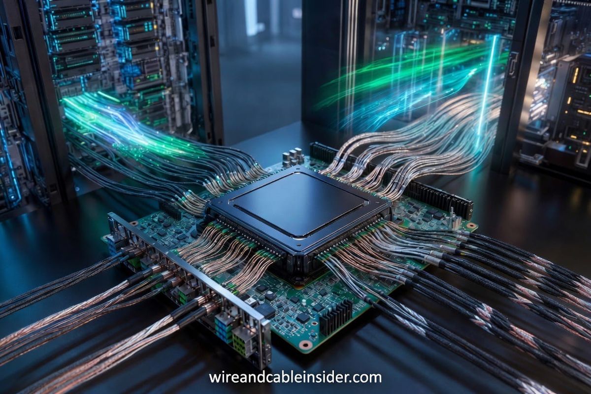
This is where near chip or Flyover Architecture, championed by companies like Samtec, provides a brilliant and highly effective solution.
Instead of relying on the circuit board to carry the data, Flyover architecture places a high density connector immediately adjacent to the processor. The signal is captured at the source and routed through ultra low skew twinax copper cable, literally flying over the PCB to the front panel or backplane.
The Engineering Advantages:
• Extended Reach: By moving the signal into twinax wire, which utilizes specialized dielectrics and precision shielding, engineers can push a 224 Gbps or 448 Gbps signal up to a full meter with incredibly low loss.
• Infrastructure Cost Savings: It allows facilities to upgrade their bandwidth capabilities using existing rack designs and standard pluggable modules like OSFP or QSFP DD without redesigning the core silicon package.
• Modularity: It retains traditional field serviceability. If an Active Electrical Cable or Direct Attach Copper cable fails, it can be easily swapped out.
Samtec has successfully proven this architecture, demonstrating 224 Gbps and prototyping 448 Gbps intra tray interconnects that bypass the PCB entirely, proving that copper wire is still a formidable force in high speed data.
Architecting the Future: On ASIC Integration
While Flyover architecture elegantly solves the immediate deployment needs, the relentless push toward 1.6T and 3.2T system levels requires engineers to look further down the horizon. When power efficiency and extreme density become the absolute primary metrics, getting close to the chip is no longer enough. The interconnect must move onto the chip.
This is the domain of On ASIC Integration, and companies like Molex are engineering the technologies that will define the future of high speed scaling.
By utilizing Co Packaged Copper and Co Packaged Optics, the electrical or optical channels are integrated directly onto the processor substrate. This eliminates almost all signal routing distance, significantly reducing the need for heavy, power hungry Digital Signal Processors.
Molex is addressing the incredibly complex physical challenges of On ASIC integration head on:
• Serviceability at the Substrate: Soldering cables directly to a high value AI processor creates a high stakes single point of failure. Molex Impress Co Packaged Copper utilizes a compression based, solderless interconnect. This protects the silicon substrate while still allowing for field replaceable rework at the chip level.
• Thermal Decoupling: In the optical realm, lasers cannot survive the heat generated by 1000W GPUs. Molex External Laser Source Interconnect System solves this by physically decoupling the laser to the front panel, keeping it cool and serviceable, while running blind mate fiber directly to the hot ASIC.
On ASIC integration is an engineering marvel that fundamentally redesigns the thermodynamic and electrical ecosystem of the server. It is built for the uncompromising future of extreme density.
The Horizon: What Exists Beyond 448G?
The networking industry rarely pauses. As 448 Gbps development solidifies, engineering task forces and standards bodies are already defining the requirements for 800 Gbps per lane, which will aggregate into monstrous 1.6 Terabit and 3.2 Terabit Ethernet connections.
At speeds approaching 800 Gbps per lane, the physics of copper wire will reach their absolute limits. The future beyond this points heavily toward:
• Silicon Photonics and All Optical Switching: Currently, data travels as light through fiber but must be converted back into electricity to be processed by a switch. Future all optical fabrics will use microscopic mirrors and photonic circuits to route light directly, eliminating the power hungry optical electrical optical conversion process entirely.
• Aerospace and Edge Deployment: These ultra dense, PCB free architectures are highly coveted in aerospace. Advanced fighter jets, radar systems, and Low Earth Orbit satellites require massive data throughput. Eliminating heavy circuit boards in favor of Flyover twinax or On ASIC optics severely reduces Size, Weight, and Power, extending battery life and lowering launch costs.
The physical layer is experiencing a renaissance. Whether utilizing advanced twinax wire to bypass the board today, or integrating optics directly onto the silicon for tomorrow, the innovation in wire and cable architecture is the quiet force making the AI revolution possible.
Disclaimer
Wire & Cable Insider is an independent, educational publication. Content is provided strictly for general informational and reference purposes. The views, thoughts, and opinions expressed in this article belong solely to the author and do not reflect the official policy, position, or views of any manufacturer, consortium, or standards body mentioned. Because application environments vary wildly, readers must verify all specifications, technical data, and safety standards independently with manufacturers before using them in live environments.